|
|
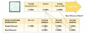
Memory – Past, Present and Future, Part 3 of 3Memories, … a foundation for inspiration. And it is inspiration, creativity and ingenuity that keep our scientist, chemist, physicist and engineers in the game. What game? The game of conceiving, developing and producing the next generation of memory chips. For the most part advances in memory technology have come from the constant and almost predictable reduction in data bit structure size. Although, it should be noted, that some of the advancements in memory technology have been structural and even procedural in nature. However, continuing to r educing the size of the transistor gate will reach the physical limit of around 10 nm and that may occur somewhere between 2010 and 2020. Listed below are technologies that will meet the growing needs until that limit is reached and also listed are other technologies that will bridge the physical limitation silicon. DUAL CHANNEL This is memory technology that was introduced by Intel in 2003 and is expected to be quickly adopted by the industry in 2004. Existing SDR DRAM and even DDR DRAM memory modules can not deliver data fast enough to keep up with current processor speeds. Shown below is the peak bandwidth of Intel P4 processors with 3 different FSB (Front Side Bus) speeds. Listed below that is the peak bandwidth of 3 different memory modules in a single channel and double channel configuration. Clearly, single channel configuration can only deliver ½ the bandwidth data requirements of today’s processor. With the introduction of dual channel technology the peak bandwidth can match current processor capacity. This technology offers additional headroom (the ability to provide more performance for future applications) with the utilization of DDR2 or QDR2 DRAM modules. http://www.kingston.com/newtech/MKF_520DDRwhitepaper.pdf
Courtesy Kingston Technology & Infineon Technologies DDR2DRAM (Double Data Rate) DDR2 is the next evolutionary step of DDR DRAM. The DDR2 technology will be based on 0.10 micron manufacturing technology and this will enable faster chips and the first modules will operate at PC400. Although current DDR technology already has modules clocked at PC 400 this may be the top end limit for the DDR technology. The PC400 is the starting point for the DDR2 series and modules released later will attain the PC533 (533MHz) and PC667 (667 MHz) clock speeds. DDR2 technology moves data twice as fast as DDR. The Common I/O DDR2 devices allow double data transfer over the I/O bus. The Separate I/O DDR2 devices provide the same DDR interface with separate input and output busses. The packaging of the DDR2 modules will differ from the standard 184 pin DDR DIMM and go to a 232 pin DDR2 DIMM package. This memory technology may not be available until 2005. http://www.qdrsram.com/presentation/QDR_Overview_Oct02.pdf
QDR2 DRAM (Quad Data Rate) This technology is fundamentally the same as DDR2 except this device delivers data 4 times as fast. The QDR 2 devices have 2 ports operating independently at twice the clock rate allowing a transfer of 4 data words in 1 clock cycle. This device will also start at PC400 and modules released later will attain the PC533 (533MHz) and PC667 (667 MHz) clock speeds. The packaging of the QDR2 modules will differ from the standard 184 pin QDR DIMM and go to a 232 pin QDR2 DIMM package. This memory technology may not be available until 2005. http://www.xbitlabs.com/articles/memory/display/qbm.html http://www.qdrsram.com/presentation/QDR_Overview_Oct02.pdf
GDDR2/GDDR3 DRAM (Graphics Double Data Rate) Graphic card manufacture heavy weights like ATI and Nvidia have jumped ahead prior to the finalization of the DDR2 standards. The GDDR2 technology is more suited for GPU (Graphic Processor Unit) with double–fetch per clock cycle, burst increment mode and special memory arrays. Wide spread adoption may be seen in 2004. Advances have continued along this line of memory technology and simples of the GDDR3 should be available this year. http://www.tomshardware.com/motherboard/20030401/ram_wars-10.html
RAMBUS XDR SDRAM (Extreme Data Rate SDRAM also known as eXternal Data Representation). This is the latest in Rambus technology. This memory module running at 3.2 GHz will deliver 8 times the bandwidth of today’s fastest PC memory. The initial modules will be clocked at 3.2GHz and later version will be clocked at 6.4GHz and possibly higher. These clock rates should enable bandwidths up to 100 Gbytes/s. This is achieved with an octal data rate where 8 data word transfers are accomplished in 1 clock cycle. Initially this memory technology will serve high bandwidth needs like graphics and networking. Eventually the technology will work its way down to PC main memory, servers, mobile systems. This technology is expected to be released in small quantities in 2004 ramping up to mass production in 2005. http://www.rambus.com/products/xdr/XDR_Controller_ProdBrief_030620.pdf
Courtesy Rambus
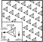
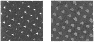
3DM RAM (3 Dimensional Memory) This memory technology deviates from the traditional planer layouts. The 3D memory structure may take one of 2 forms. First, a 3D memory module could have the memory bit structure laid out in a planer fashion just as the conventional memory chip; however, in a 3D module there would be multiple layers stacked on top of each other to form a 3D structure. The 2nd approach would be to fabricate the memory bit structures in a vertical plane. Maxtrix Semiconductor has taken the lead in this technology and has produced some products in 2003 and may manufacture larger commercial quantities in 2004. http://www.sciam.com/article.cfm?articleID=000BD05C-D352-1C6A-84A9809EC588EF21
Courtesy David Scharf
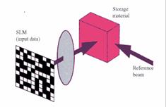
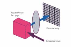
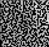
HDSS (Holographic Data Storage System) Holographic technology is coming of age and we will soon see it in the marketplace. A holographic crystal the size of a sugar cube could store 1 terabyte (TB) of data. The holographic process involves splitting a laser light into two beams. One beam is modulated with data and the other beam remains unaltered. Both beams are redirected through a photosensitive crystal in such a manner that they crisscross. Where the beams crisscrossed they will create an interference pattern (amplitude mixing of the two waveforms). This interference pattern alters the optical medium by changing the absorption, refractive index or thickness of the media at a specific spot the size of the laser beam. Additional data can be recorded in the same spot by pointing the laser with a slightly different angle. Many different angles can be used to record data in the same spot. Further multiplexing is accomplished by changing the laser wavelength and repeating the process on the same spot. So one small spot the size of a laser beam cross section can contain a vast amount of data and this process is repeated throughout the total volume of the media. The data crystal is read by shining a reference laser into the crystal and the image is projected onto a CCD (Charge-Coupled Device) which converts the light and dark areas into 1s and 0s. IBM has lead the R&D work in HDSS and this technology is due for commercial release but an availability date has not be set. www.research.ibm.com/journal/rd/442/ashley.html
Write Read Image
Courtesy IBM
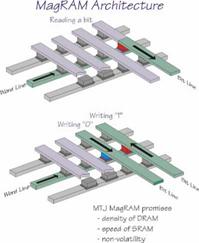
MRAM ( Magnetic RAM also known as Magnetoresistive RAM). This is an exciting new concept in memory technology. Heretofore, all RAM has been based on the storage of electrons. MRAM stores data not by electron charge but by the electron spin that is held in a magnetic sandwich otherwise known as magnetic tunnel junction. MRAM will offer the best of the 3 families of memory. MRAM will have the density of DRAM, the speed of SRAM and the non-volatility of Flash RAM. The speed as mentioned earlier is 30 times faster than DRAM and other benefits include low power for mobile devices. 4Mbit sampling chips were available in 2003 and volume production of 256 Mb chips is expected in 2004. The immediate market for this technology appears to be cell phones, PDA, digital camera and MP3 players along with other typical mobile devices. Eventually this technology will work its way down to the PC main memory market. http://neasia.nikkeibp.com/nea/200207/cmpo_193844.html
Courtesy IBM
FeRAM or FRAM (Ferroelectric RAM) this technology is a fast random access non-volatile storage. This RAM is capable of typical read speeds but it has a much faster writing speed than is available with Flash memory and could eventually replace Flash memory. FeRAM is composed of ferroelectric crystal capacitor placed in a grid on a silicon substrate. Memory function of switching between a 0 and 1 is accomplished by applying an electric field to the crystal. This causes a ‘central’ atom to move toward the field. When the field is removed the ‘central’ atom remains in the new location. The position of the ‘central’ atom affects the voltage which is used to determine whether it represents a 0 or a 1. Small 1 Mb samples were available in 2001 using 0.5 micron fabrication and 4 Mb samples using 0.35 micron fabrication were available in 2002. 16 Mb samples using 0.25 micron technology were available in 2003 and 64 Mb samples using 0.18 micron technology are expected in 2004. 128 Mb using 0.18 micron technology is expected to appear in 2005 and the 256 Mb modules are expect to follow. http://neasia.nikkeibp.com/nea/200110/cmpo_145693.html
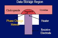
OUM RAM (Ovonic Unified Memory) This is a non-volatile semiconductor memory technology. This technology is based on the CD-RW and DVD-RW phase change technology. A thin film layer of Chalcogenide is laid down over an electrode in the bit cell structure. During a write process the electrode heats the thin film metal surface into an amorphous state (no crystal structure) which changes the conductivity of the metal. The differences between these two levels of conductivity represent the 1 and 0 of a bit function. The bit can be erased with a lower temperature setting that caused the thin film metal to become plastic and then as the metal cools it crystallize into its original form which produces a different level of conductivity. OUM RAM offers small, scalable fast write low voltage and low process cost chips. Faster write and erase speeds, higher cycle endurance than Flash memory. No availability time line data was found. http://www.ovonic.com/news_events/5_2_press_releases/20030205.htm
Courtesy Intel
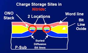
NROM (Nitrated ROM also know as Nitride MOS) is somewhat similar to CMOS (Complementary Metal Oxide) semiconductor except part of the bit memory structure is comprised of nitride oxide. This compound demonstrates better physical and electrical properties than CMOS technology but it had previously been difficult to manufacture and these difficulties have been overcome. Currently, Intel’s multilevel approach stores 2 bits per cell by using 4 levels of charge. (This technology is not easily scalable to 4 bits per cell because it would require 16 levels of charge). AMD and Fujitsu multi-bit approach stores 2 bits per cell by trapping 2 pockets of electrons in a nitride layer under a bidirectional gate. So to get 4 bits per cell AMD, Fujitsu and Saifun will combine the multilayer and multi-bit technologies by putting 4 levels of charge in each of the 2 bit location in each cell. With more development the NROM may compete with the magneto-resistive Ram, ferroelectric RAM, Ovonic memory and some polymer based devices. AMD, Fujitsu and Saifun Semiconductors are moving forward with a 4 bit per cell chip in 2004. http://www.eetimes.com/story/OEG20020802S0061
Courtesy Intel
Molecular RAM This approach is another promising memory technology that is working its way through the R&D labs. This technology involves placing a disk shaped organic molecule called porphyrins in a row on an electro-active surface. A small voltage is applied which causes the molecule to lose an electron and change state. The ‘on’ and ‘off’ state is read by the CPU. Each molecule can store 3 bits at each location and this gives each location 8 possible states. i.e., 2^3 = 8. This molecule has been tested at 400 degrees C and over 1 trillion cycles indicating they are stable for real world environments. The small size facilitates high capacity and fast access times. R&D work is continuing on this technology and competitive RAM modules should be available in 10 years. http://www.nanoelectronicsplanet.com/nanochannels/research/article/0,4028,10497_3116371,00.html
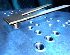
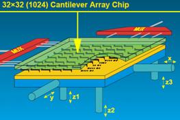
Courtesy HP
Plastic ROM This is a plastic polymer known as PEDOT which conducts electricity at low voltages but operates as a semiconductor in high voltages. Bits are written when a current passes through a polymer fuse causing it to blow and change its conductivity. The difference in the conductivity represents a 1 or 0. Unfortunately this technology can only be written once but can be read many times. This is a cheap high capacity solution for camera, MP3 players and other mobile devices. No indication when this technology will be commercially available. http://www.internetnews.com/infra/print.php/3108941 Probe RAM This is a memory technology currently under development by IBM and a few others. Probe memory technology stems from the advancements made in the microscope industry. Research in probe memory technology may acquire stylus techniques from STM (scanning tunneling microscope), FEP (Field emission probe) or AFM (Atomic force microscope) However; IBM’s millipede is a little different but falls under a general classification of probe memory. The millipede chip consists of a layer of Plexiglas only a couple of billionths of an inch thick laid down on a silicon substrate. To write a bit a microscope tip heats to 750 degrees F and softens the Plexiglas and then dents it. To read the bit the tip is heated to 570 degrees F (which is not enough to soften the Plexiglas) and the tip is then pulled across the surface. When it falls into a dent the tip cools, because it comes in contact with the sides of the pit which is cooler than the tip. As the tip cools it reduces the electric resistance and this is measured. The data can be erased by passing the hot tip over the dent and it softens the Plexiglas which becomes plastic and flows to fill the dent. The read speed of a single probe is 1000 times slower that a hard drive and to speed the operation the millipede chip is fabricated with 1024 silicon tips that are read in parallel. IBM reports they have achieved 1 trillion bits per square inch. The technology is promising but it will take as much as 10 more years of R&D before this technology will become commercially viable. http://www.research.ibm.com/resources/news/20020611_millipede.shtml
Courtesy IBM
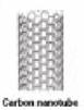
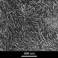
Nanotubes RAM This is a non-volatile memory technology using carbon nanotubes. Nantero, based in Boston, appears to be making significant progress in this field. Instead of growing nanotubes in a specific orientation, Nantero grows nanotubes over the entire silicon surface and then uses existing lithographic equipment to etch away nanotubes that are not in the correct alignment. A pair of electrodes are arranged across the remaining nanotubes. A small electric field alters the tube so that they bridge the gap between the electrodes and this changes the conductivity. These two states of different conductivity represent the binary 1 or 0. The benefit of nanotube RAM is that it is considerable faster and denser than DRAM, substantially lower power consumption then DRAM or Flash and resistant to environmental forces like heat, cold and magnetism. Nantero expects to have a 4 Mbit sample in 2004 and competitive RAM sizes by 2007. http://www.impactlab.com/modules.php?name=News&file=article&sid=2402
NVQDM RAM (Non-Volatile Quantum DotMemory) This is a non-volatile RAM technology. A number of companies have on going R&D programs in this field because of the potential this field offers to data storage and processor performance. Some estimates indicate as many as 1.1 trillion dots could be placed in 1 square inch of special semi-conducting material. That is the equivalent storage of 200 movies in the area the size of a postage stamp. The basic technology is to fabricate a structure 15nm square in size. The binary effect is achieved by the presence of an electric charge within the dot. Fujitsu in a process called quantum dot wavelength multiplexed memory has developed an interesting way of reading and writing data to the quantum dots by using a laser. The technique offers very fast write speeds of 5 nano second/bit or the equivalent of storing a 2 hour movie in just 3 minutes. This technology may be commercially available in 6 years. http://magazine.fujitsu.com/us/vol34-2/paper05.pdf
Courtesy Fujitsu NEXT MONTH An addendum, (Part 4) will be added to this series and it will be dedicated exclusively to memory sizing and performance. All ‘Baby Steps to our Future’ articles are archived at www.hal-pc.org/~seeker/future. |
2004 Ron Fenley worked as an engineer/analyst and retired in 1999. Ron moved to the country and now pursues his interest in computers, basic science and technology. Ron has been a computer enthusiast for 20 years and has been a HAL-PC member for about half that time. Ron can be reached at future@hal-pc.org
|