|
|
Memories,. the fabric a lifetime has made.As a child, one has a huge capacity for memory storage and a child fills that vessel quickly as they experience life's adventure. As for some others, that vessel seems to have filled to the brim and is leaking at the seams. For some people, like this author, it is leaking profusely. It is unfortunate human memory can't be refreshed like computer memory. There are some types of computer memory that leak profusely and have to be refreshed hundreds of times a second. There are others that retain the data for a lifetime. Each has carved a niche in the electronics world. Long gone are the days of Core Memory, which was the first random accessible memory for a computer. That memory of olden days was composed of small ferrous donut rings with two wires running through the center of each that formed a grid of memory cells. This antique was bulky, heavy and had a nasty 'feature' of losing the data every time the data was read; yet, it was still a great advancement over punched cards or tapes. We have come a long way since then and there have been just two dozen types of memory developed over the 25 years since core memory. In Part 1 of this series we will look at the baby steps of development that the semiconductor chip has taken over its evolution.
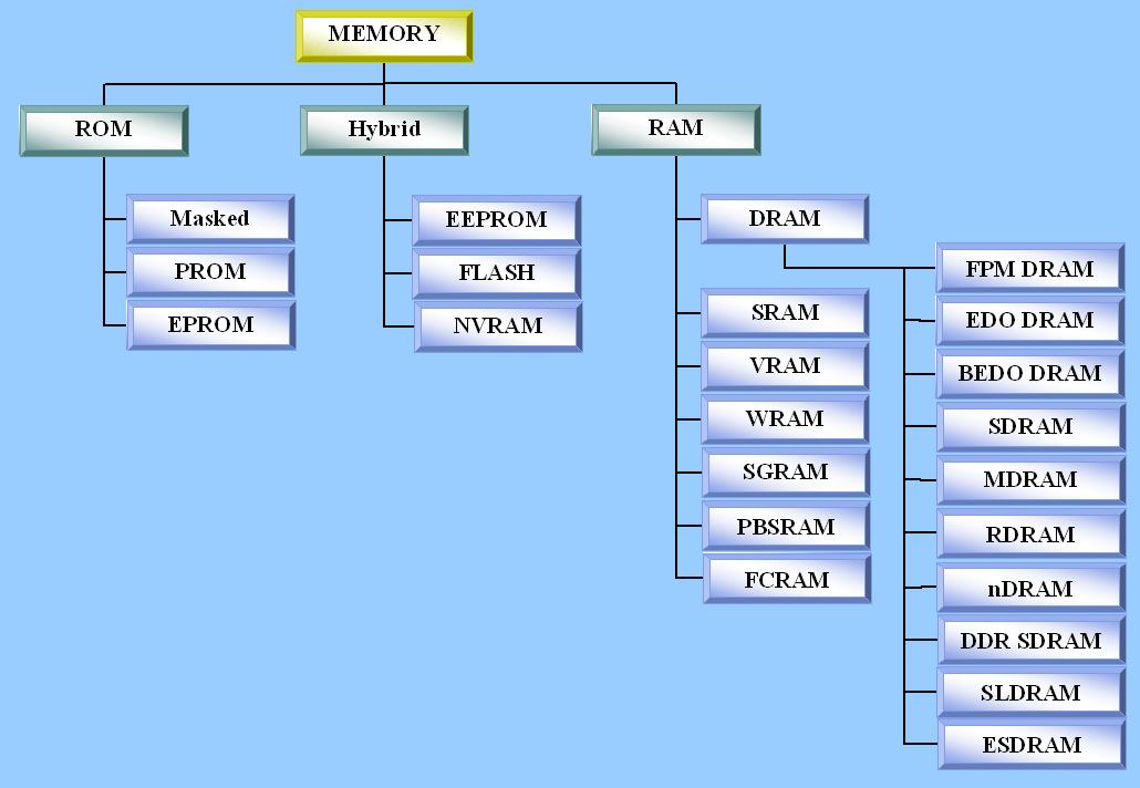
Memory Types Fundamentally, there are three families of memory, Read Only Memory (ROM), Random Access Memory (RAM) and a Hybrid . Table 1 illustrates the three families and most of their members.
ROM By design, ROM will not lose the data value when the power is removed. ROM is a write-once read-many non-volatile type memory. Later developments in ROM technology did permit re-writing of the ROM chip but it required special handling. Masked ROM This is a non-volatile data chip where the data configuration is encoded directly on the silicon during the fabrication process. This type of device is designed to perform a specific function and clearly cannot be changed. Because of the re-writing limitation this device is limited to small well-established programs used to interface with hardware. Printers would be an example of where Masked ROM would be used. PROM - Programmable Read Only Memory . This is a non-volatile ROM chip that can be programmed using a special piece of equipment called a PROM Programmer that 'burns' the data onto the chip memory. Data programmed into the chip can be written only once and like the masked ROM it cannot be changed. The capability of loading your own program data on-site makes this device more popular than the masked ROM, but it is more expensive. EPROM - Erasable Programmable ROM . This is a non-volatile ROM chip that can be erased and reprogrammed. Each chip has a small quartz window installed in the top of the ROM package, through which you can see the chip that holds the memory. A specific frequency of ultraviolet light can be shined through this window to erase the EPROM where it can be reprogrammed using a PROM Programmer. An EPROM without this quartz glass window is called OTPROM (One-time PROM). These are quite useful during software development because the program can be loaded into the EPROM and tested and then the process can be repeated multiple times, until the program is finalized. The disadvantage is that the chip has to be removed from the test circuit to be reprogrammed. HYBRID Hybrid memory blends the non-volatile capability of ROM and the read/write capability of RAM. With a Hybrid memory one is able to read/write to the module and the data is retained once the power is removed from the chip. EEPROM - Electrically Erasable Programmable ROM. This is a non-volatile data chip that can be erased and re-written under software control. EEPROM is the most flexible of the ROM types and is now commonly used for holding hardware BIOS programs. The memory can be selectively erased one byte at a time and this chip does not have to be removed from the circuit to be reprogrammed. This type of chip is widely used to hold hardware interface programs called Basic Input Output System (BIOS). These are commonly found in system boards, modems, video cards, SCSI cards, etc. FLASH Memory. This is a non-volatile data chip that is electrically erasable and re-writable. The word "flash" refers to the ability to erase and write a volume of memory electrically. With Flash memory a 512 byte block of memory can be written or erased at one time which makes it faster than the one byte at a time EEPROM. Another advantage is the cell configuration is simpler than EEPROMs, so it can handle a massive amount memory with low-power consumption. One disadvantage is that Flash memory has a lower number of rewriting cycles. This type of memory is widely used in portable electronics. NVRAM - Non-Volatile RAM . This is any type of memory that is made non-volatile by connecting a constant power source, such as a battery. This type of memory does not lose its data when the main power is turned off. A typical application of this type of memory would be the CMOS memory in a computer system. A small chip of perhaps 64 bytes has a very small battery attached that trickle charges a small voltage to the chip to maintain the data state once the main power supply is turned off. RAM RAM is a read/writeable volatile memory chip. By far this is the most common family of memory in use today. This chip permits unlimited read/writes, but the down side is the data is lost when the power is removed. RAM chips are much faster than ROM chips due to the nature of how information is stored. RAM is often used to shadow hardware BIOS to improve performance when executing BIOS code. There are several different types of RAM, and many variations of DRAM. DRAM - Dynamic Random Access Memory . This is the largest and most popular type of memory with several variations. DRAM consists of a transistor and small capacitor for each bit of memory. When the capacitor is energized it represents a "1" and no charge represents a "0". The transistor is used to read the contents of the capacitor. These are tiny, low capacity high-speed capacitors and they can only hold a charge for a short period of time. This memory will only hold data if it is refreshed with a special logic called a refresh circuit and this circuit must cycle hundreds of times a second. This action of refreshing is why the chip is called Dynamic RAM. Also, the process of reading the contents of the memory is destructive, meaning extra time must be spent restoring the contents of the memory addresses that have been accessed. DRAM was generally replaced by FPM DRAM. FPM DRAM - Fast Page Mode DRAM . This type of DRAM memory is faster than previous generation DRAM. The speed was achieved by working within a page of memory. Memory is laid out in Rows and Columns. A page is described as the section of memory at a specific row address. Within one specific row are several columns of memory bits. The row address can be specified just once to make multiple column reads within the same page address. Successive reads to the same page of memory only require the column address to be changed, which saves time in accessing the memory. FPM DRAM was generally replaced by EDO DRAM. EDO DRAM - Extended Data Output DRAM also known as Hyper-Page Mode . This type of DRAM can start fetching the next block of memory at the same time that it sends the previous block to the CPU making it up to 25% faster than standard DRAM. EDO DRAM works similarly to FPM DRAM by addressing page memory. The primary advantage of EDO DRAM is that it holds the data valid even after the column strobe signal goes inactive. While the EDO DRAM is retrieving data for the microprocessor, the microprocessor can perform other tasks and the EDO DRAM will maintain the data integrity. This type of memory has an internal cache, which allows for an entire block of memory to be read at once. This type of transfer is called a pipeline burst. EDO DRAM is only slightly more expensive than conventional DRAM. EDO DRAM is being replaced by SDRAM in newer computer systems. BEDO DRAM - Burst Extended Data Output DRAM . This type of DRAM can process 4 memory addresses in 1 burst. Also, it can send data to the processor from a read operation and at the same time read-in the address of the next data to be sent. Once the new data address has been read, it can send the data in burst- mode in three successive clock cycles without clock coordination, yet it can stay synchronized with the processor for a short burst period. This type of DRAM works well with the Front Side Bus (FSB) speed up to 66 MHz. This type of memory is slightly faster than EDO DRAM, because of the burst mode. However, many system board manufactures did not offer support for BEDO DRAM opting for the newer SDRAM and this RAM has become obsolete. SDRAM - Synchronous DRAM . This type of Single Data Rate ( SDR ) DRAM is synchronized with the Front Side Bus ( FSB ) clock. The SDRAM data input and output is synchronized to this external clock where FPM, EDO and BEDO DRAM were driven by a signal that actives the chip. Synchronized by the FSB clock allows for extremely fast consecutive read and write capability over all previous types of DRAM. Additionally, this chip incorporates interleave technology where the CPU can make reads to multiple memory address simultaneously. Name variations from new generations of SDRAM may be seen as PC66, PC100, PC133,PC2100, etc., each of which meets the respective specification from Intel Corporation. The SDR SDRAM chips are gradually getting replaced with the DDR SDRAM chips, although, SDRAM is still widely in use. MDRAM - Multi-bank DRAM . This is a DRAM that is specifically used in graphics cards. Conventional memory designs use a single monolithic "block" of memory for the frame buffer. MDRAM breaks up this memory into multiple 32 KB banks that can be accessed independently. This provides flexibility in memory sizing. Previously, video cards with conventional video RAM memory had been sized in whole increments like 1MB, 2MB, 4MB, etc. If you produced a video card to run at 1024x768 resolution in true color (24 bits), it would require 2.25 MB of video memory. With conventional memory, the smallest unit that would work would be a 4 MB module where with MDRAM a 2.25 MB of memory could be created. MDRAM is also more cost-effective to manufacture compared to VRAM and it runs slightly faster than VRAM. RDRAM - Rambus DRAM . This is a DRAM that was first used in video cards under the name Base Rambus or Concurrent Rambus . Rambus DRAM currently used in the main memory market is known as Direct Rambus . This chip uses a 16 or 18 bit data path and supports up to 4 channels. RDRAM was designed to be synchronized with the FSB and produce a burst data rate of 1.6 GHz. Currently, RDRAM is only used in certain high-performance graphics workstations, servers and it is also used in the Nintendo64. Intel licensed RDRAM technology for some of its motherboards, but has since pulled back somewhat on its RDRAM development efforts. Name variations may be found as PC400 or PC800 RDRAM nDRAM - Intel and Rambus were working on a new version of RDRAM, called nDRAM, that would support data transfer speeds at up to 3.1Gb/s. Not a great volume of new information is available which might suggest they have scaled back or discontinued their R&D efforts. DDR SDRAM - Double Data Rate (DDR) Synchronous DRAM . This type of SDRAM runs twice as fast as traditional SDRAM by transferring data on both edges of the clock cycle. Additionally, this chip incorporates interleave technology where the CPU can make reads to multiple memory address simultaneously. DDR SDRAM is becoming quite popular over the standard SDR SDRAM and may eventually replace it completely. Additional name variations from new generations of DDR SDRAM may be seen as PC2100, PC2700, PC3200, PC4200, etc each of which meets the respective specification from Intel Corporation. SLDRAM - Synchronous Link DRAM . This type of DRAM uses a multiplexed-bus to transfer data on a few pins rather than multiple fixed pin settings, thus achieving a higher bandwidth on each pin. A consortium of computer vendors were working on this type of DRAM as an alternative memory architecture to RDRAM, although, this technology now appears to be obsolete. ESDRAM - Enhanced Synchronous DRAM . This DRAM chip overcomes some of the inherent latency problems with standard DRAM by including a small amount of SRAM (described later) onto the chip, which effectively crates an on-chip cache. The processor accesses the fast SRAM which has a lower latency time and burst operations up to 200 MHz. The internal data channel between the DRAM and SRAM is large allowing fast data transfers. EDRAM - Enhanced DRAM is the non-synchronized version of this technology. SRAM - Static RAM. This type of RAM holds data without external refreshing and maintains data integrity for as long as power is supplied to the circuit. This type of memory is faster and more reliable than DRAM because it does not need to be refreshed as often, but it is more expensive and requires more power. SRAM is used for Level 1 and Level 2 cache memory because of the speed this chip offers. Each SRAM bit is comprised of four to six transistors, which is why SRAM takes up much more space compared to DRAM, which uses only one transistor and one capacitor. VRAM - Video RAM. This is a video version of the FPM DRAM memory that is used in video adapters. With ordinary DRAM, the CRT and CPU must compete for a single data port, causing a bottleneck of data traffic. VRAM is a dual-ported memory that solves this problem by using two separate data ports. One port is dedicated to the RAMDAC (Random Access Memory Digital Analog Converter), for refreshing the CRT and updating the image on the screen. The second port is dedicated to the CPU or graphics controller for changing the image data stored in memory. VRAM is generally replaced by RDRAM and WRAM WRAM - Windows RAM. This is very similar to VRAM but it supports EDO technology. This RAM technology also supports dual porting with one port dedicated to the RAMDAC (Random Access Memory Digital Analog Converter), for refreshing CRT and updating the image on the screen. The second port is dedicated for to the CPU or graphics controller for changing the image data stored in memory. WRAM was developed later and is faster and less expensive. SGRAM - Synchronous Graphic RAM . This is a single port DRAM designed for graphics hardware that requires high-speed throughput such as 3-D rendering and full-motion video. This type of memory can be considered a graphic-optimized version of SDRAM containing several read/write functions dedicated to graphic processing. SGRAM, uses certain techniques like retrieving data in blocks to provide more bandwidth to graphics-intensive operations. This type of RAM is also synchronized to work with the system bus. PGSRAM - Pipeline Burst Static RAM. The PBSRAM chip has input and output registers for data, which are not incorporated into the flow-through device. This allows the pipelined device to operate with a much faster cycle time than the flow-through version. FCRAM - Fast Cycle RAM. This RAM is fabricated with memory array segmentation and internal pipelining that speed random access and reduce power consumption. This type of RAM is intended for specialty application such as high-end servers, printers and telecommunications switching systems. References
Next Month In Part 2 of this series we will look at Parity, Non-parity and ECC memory, Sizing & Performance, Memory Systems and several other items. In Part 3 we will look at new memory technology that may produce the memory chips of the future. |
2004 Ron Fenley worked as an engineer/analyst and retired in 1999. Ron moved to the country and now pursues his interest in computers, basic science and technology. Ron has been a computer enthusiast for 20 years and has been a HAL-PC member for about half that time. Ron can be reached at future@hal-pc.org
|